N-type Semiconductor
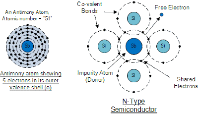
This permits four out of the five orbital electrons to bond with its neighboring silicon atoms leaving one “free electron” to become mobile when an electrical voltage is applied (electron flow). As each impurity atom “donates” one electron, pentavalent atoms are usually called “donors”.
Antimony (symbol Sb) as well as Phosphorus (symbol P), are often used as a pentavalent additive to silicon. Antimony has 51 electrons arranged in five shells around its nucleus with the outermost orbital contains five electrons. The resulting semiconductor basics material contains an excess of current-carrying electrons, each with a negative charge, and is therefore referred to as an N-type material with the electrons are known as “Majority Carriers” while the resulting holes are known as “Minority Carriers”.
Stimulating by an external power source, electrons are released from the silicon atoms and quickly replaced by the free electrons available from the doped Antimony atoms. But this action still leaves an extra free electron moving around the doped crystal creating it negatively charged.
Then a semiconductor material is classified as N-type when its donor density is greater than its acceptor density, in other words, it has more electrons than holes thereby creating a negative pole as shown.
Antimony Atom and Doping
N-type (Doping by Antimony)
Materials added with
Pentavalent impurity atoms (Donors) and accompanied by “electron”
movement are known as N-type Semiconductors. Following things happened
in N-type semiconductors:
- Positively charged donors.
- Huge number of free electrons.
- Very few holes in comparison to free electrons.
- Doping provides:
- Donors with positively charged.
- Free electrons with negatively charged.
5. Energy supply provides:
- negatively charged free electrons.
- positively charged holes.
P-Type Semiconductor
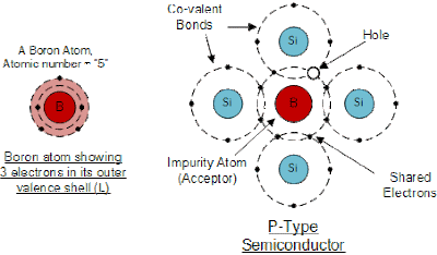
The fourth closed bond cannot be formed if a "Trivalent" (3-electron) impurity is introduced into the crystalline structure, such as Aluminum, Boron, or Indium, which only have three valence electrons accessible in their outermost orbital. As a result, a complete connection is not feasible, resulting in an abundance of positively charged carriers known as holes in the crystal structure where electrons are essentially missing, giving the semiconductor material an abundance of positively charged carriers known as holes.
Because of having a hole in the silicon crystal, a neighboring electron is attracted to it and will try to travel into the hole to fill it. However, the electron filling the hole leaves another hole behind it as it travels. As a result, this attracts another electron which in turn creates another hole behind it, and therefore giving the presence that the holes are travelling as a positive charge through the crystal structure (conventional current flow).
Because to the displacement of holes, there are less electrons in the silicon, causing the entire doped crystal to become a positive pole. Trivalent impurities are known as "Acceptors" because they are constantly "accepting" extra or free electrons because each impurity atom causes a hole.
Boron (symbol B) is a frequent trivalent additive because it contains only five electrons distributed in three shells surrounding its nucleus, with only three electrons in the outermost orbital. Boron atom doping enables conduction to be dominated by positive charge carriers, resulting in a P-type material, with positive holes referred to as "Majority Carriers" and free electrons as "Minority Carriers."When the acceptor density exceeds the donor density, a semiconductor basic material is classified as P-type. A P-type semiconductor has more holes than electrons as a result.
Boron Atom and Doping
P-type (Doping by Boron)
Materials added with Trivalent impurity atoms (Acceptors) and accompanied by “hole” movement are known as P-type Semiconductors. Following things happened in this type of materials:
- Negatively charged acceptors.
- Huge number of holes.
- Very few free electrons compare to the number of holes.
- Doping provides:
- Acceptors with negatively charged.
- Holes with positively charged.
5. Energy supply provides:
- positively charged holes.
- negatively charged free electrons.
Overall, both P and N-types are electrically neutral on their own. Antimony and boron are two doping agents that are more commonly available than other materials. They are also known as "metalloids". There are a number of other chemical elements that share the same three- or five-electron outer-shell configuration, which makes them good choices for doping materials in the periodic table. Other elements can also be used to dope a base material of either silicon or germanium to produce different types of basic semiconductor materials for use in electronic semiconductor components, microprocessors, and solar cells.

