Gate Driving Techniques for High-Speed MOSFET Applications

This article explores the principles, techniques, and best practices for driving MOSFETs in high-speed applications, with emphasis on circuit design, component selection, and signal integrity.
1. Introduction to Gate Driving
The MOSFET gate behaves like a capacitive load that needs to be charged and discharged quickly to switch between ON and OFF states. In high-speed switching (e.g., in SMPS, motor drives, Class D amplifiers), the gate driver’s job is to provide fast, powerful voltage transitions to overcome the gate capacitance swiftly without ringing or overshoot.
2. MOSFET Gate Characteristics
The input gate of a MOSFET is modeled by:
-
Gate-source capacitance (Cgs)
-
Gate-drain capacitance (Cgd) — also called Miller capacitance
-
Gate charge (Qg) — the total charge needed to switch ON or OFF
To turn the MOSFET ON, the driver must supply a gate voltage (Vgs) above the threshold voltage (Vth) and enough current to move the gate charge in a very short time:
Where:
-
= gate charge (nC)
-
= desired switching time (ns)
3. Key Parameters in High-Speed Switching
To optimize high-speed performance, consider the following:
| Parameter | Description |
|---|---|
| Rise/Fall Time | How quickly Vgs reaches required level |
| dv/dt and di/dt | Switching speed, affects EMI and losses |
| Gate Charge (Qg) | Affects driver current requirement |
| Rg (Gate Resistance) | Controls switching speed and EMI |
| Miller Plateau | Affects switching loss and timing |
4. Gate Driver Architectures
4.1 Discrete Gate Drivers
Using BJTs, MOSFETs, or complementary pairs (Totem Pole) to construct a driver manually. Offers flexibility but is less efficient and compact.
Pros:
-
Customizable
-
Good for prototyping
Cons:
-
Complex
-
More board space
4.2 Integrated Gate Driver ICs
These are dedicated ICs designed to drive high-side or low-side MOSFETs.
Common features:
-
High output current (up to ±4A or more)
-
Fast rise/fall times
-
Built-in dead-time control
-
Under-voltage lockout (UVLO)
-
Shoot-through protection
Examples:
-
IR2110, IRS2186 (Infineon)
-
TC4420/TC4422 (Microchip)
-
UCC27424, UCC21520 (Texas Instruments)
5. Gate Resistor Selection
Gate resistor (Rg) is critical in controlling the switching speed, damping oscillations, and managing EMI.
Guidelines:
-
Use low values (2–10Ω) for fast switching
-
Use higher values (10–100Ω) to reduce EMI or overshoot
-
Consider split Rg for tuning rise and fall times separately
Tip: Always observe waveforms using an oscilloscope to fine-tune the resistor.
6. Protection and Isolation Techniques
a. Shoot-Through Protection
Occurs when high-side and low-side MOSFETs conduct simultaneously. Mitigation:
-
Dead-time insertion
-
Cross-conduction logic in drivers
b. Under-Voltage Lockout (UVLO)
Prevents driving the gate when Vcc is below a safe threshold.
c. Isolation
In half-bridge/full-bridge or high-side configurations, galvanic isolation is needed:
-
Opto-isolators
-
Digital isolators
-
Transformers
7. Bootstrap Circuitry for High-Side Driving
Driving a high-side n-channel MOSFET requires a voltage above the source, which changes dynamically. Bootstrap circuits are an efficient solution.
Components:
-
Bootstrap diode (fast-recovery type)
-
Bootstrap capacitor (typically 0.1μF to 1μF)
Operation:
-
When the low-side MOSFET is ON, the bootstrap cap charges.
-
When the low-side switches OFF and high-side turns ON, the cap provides gate drive voltage.
8. Practical Considerations
-
Minimize loop inductance: Use short, wide PCB traces
-
Use decoupling capacitors: Close to driver supply pins
-
Thermal management: High switching frequency increases power loss
-
Check datasheets: Ensure voltage ratings and drive strength match MOSFET specs
9. High-Speed MOSFET Gate Driver with Bootstrap Circuit
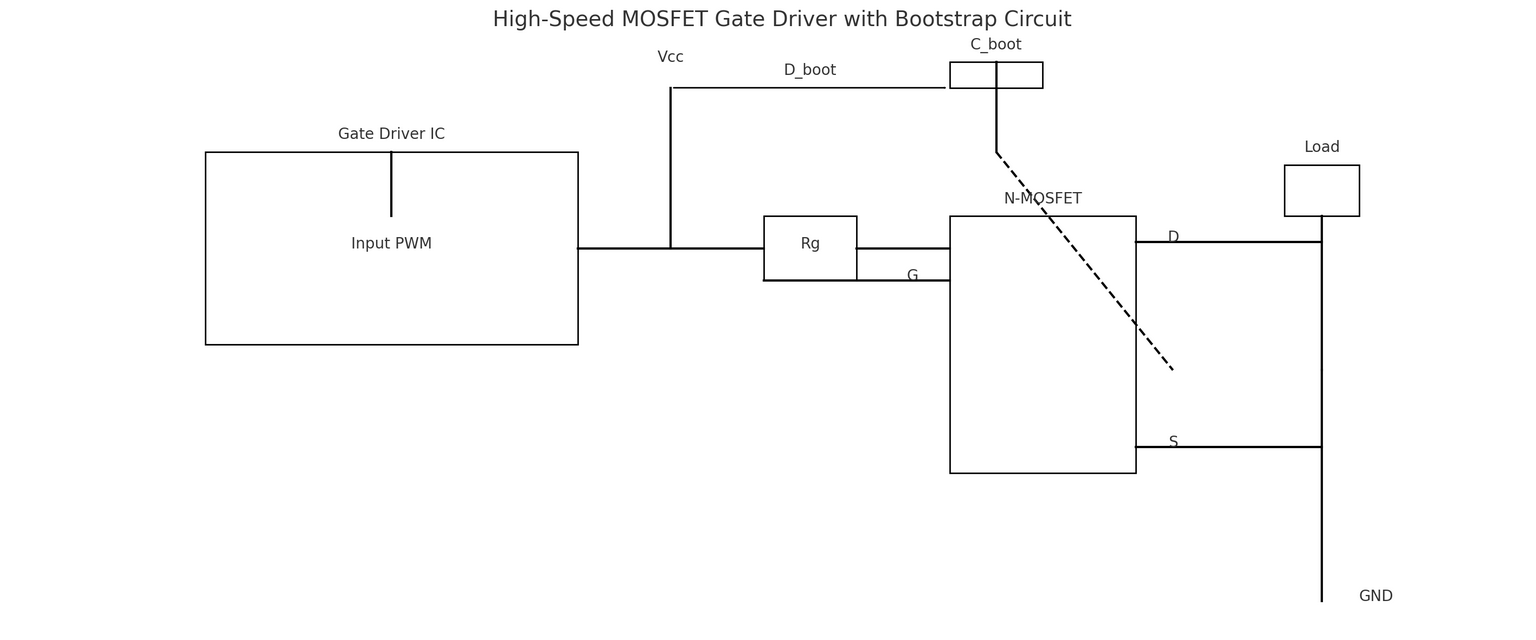
Components in the Diagram
-
-
Accepts a low-power PWM control signal (e.g., from a microcontroller)
-
Amplifies this signal to a higher current/voltage level (typically 10–15V) to drive the MOSFET's gate
-
-
Gate Resistor (Rg)
-
Limits inrush current into the MOSFET gate
-
Controls switching speed and suppresses ringing
-
-
N-Channel MOSFET
-
Acts as a switch controlling power to a load
-
High-side or low-side depending on the configuration
-
-
Bootstrap Diode (D_boot)
-
Allows current to flow only from Vcc to charge the bootstrap capacitor
-
-
Bootstrap Capacitor (C_boot)
-
Stores charge used to supply gate voltage for the high-side MOSFET
-
Provides voltage above source (Vgs > Vth) for MOSFET turn-on
-
-
Load
-
Connected in series with the MOSFET
-
Could be a motor, inductor, or resistive load
-
Working Principle
Step 1: Initialization
-
When the low-side MOSFET is ON (or when source is at ground), the bootstrap capacitor (C_boot) charges through the bootstrap diode (D_boot) from the Vcc supply.
-
This ensures that the capacitor is holding a voltage close to Vcc.
Step 2: Turning ON the High-Side MOSFET
-
To turn ON the high-side N-channel MOSFET, the gate voltage must be higher than the source by at least the threshold voltage (Vgs > Vth).
-
The gate driver uses the charge stored in the bootstrap capacitor to create a voltage that is Vcc above the source (which is now rising), allowing proper MOSFET conduction.
Step 3: Switching
-
The gate driver turns the MOSFET ON and OFF rapidly based on the PWM input.
-
The gate resistor slows down the rise and fall times to control EMI and reduce ringing.
Step 4: Recirculation
-
Once the MOSFET turns OFF, the source returns to ground potential, allowing the bootstrap capacitor to recharge through the diode in the next cycle.
Key Considerations
-
Bootstrap capacitor value must be sufficient to supply the gate drive during ON-time without discharging too much.
-
Diode speed must be fast recovery type to handle high-speed switching.
-
Dead-time control is essential to avoid shoot-through in full-bridge or half-bridge topologies.
10. Frequently Asked Questions (FAQs)
Q1: Why can't I drive a MOSFET gate directly from a microcontroller?
A: Most microcontrollers cannot source/sink enough current (typically <20mA) to charge/discharge the gate capacitance quickly. This results in slow transitions, increased switching loss, and potential overheating.
Q2: What is the purpose of a gate resistor?
A: It controls the switching speed, limits inrush current, and damps ringing caused by parasitic inductance and capacitance.
Q3: Can I use a p-channel MOSFET for high-side switching?
A: Yes, but p-channel MOSFETs have higher ON-resistance and lower speed compared to n-channel. N-channel with a bootstrap driver is preferred for efficiency.
Q4: What causes gate ringing, and how do I suppress it?
A: Ringing is caused by LC oscillation between the gate capacitance and stray inductance. Suppress it with:
-
Gate resistors
-
Proper PCB layout
Q5: How much current should my gate driver provide?
A: It depends on total gate charge (Qg) and desired switching time (t_sw):
For instance, a MOSFET with 40nC Qg and 20ns desired switch time needs a driver capable of at least 2A.
11. Conclusion
Efficiently driving a MOSFET gate in high-speed applications requires a deep understanding of gate charge behavior, switching dynamics, and driver circuit design. Whether using a discrete or integrated driver, key elements like bootstrap circuits, gate resistors, dead-time, and isolation must be carefully implemented to ensure reliable, high-performance operation.
By following sound engineering principles and selecting components appropriately, engineers can unleash the full potential of MOSFETs in advanced power electronics systems.
Join the conversation